I think it’s about time to get me a logo for the DWMC-16 project, and I had the idea to get me a front from or looking like it’s from the 70s and then simply write out ‘DWMC-16’ to use as a logo. And I think it looks quite nice.

First Schematics: 16 bit Register
Basic Flip Flop
I’ve had the idea to set down the first schematics for the 16 bit Register for a while now, but I’ve been looking for a usable and simple tri-state logic output, so that I can select the output. The same goes for the input, which needs a write enable to be usable. Finally, I’ve found something and I believe that I might have something workable.

The Flip Flop itself is more or less just a simple bog standard bistable transistor logic, which can be set and reset by Q6. The idea is pretty much taken from this Creative Engineering blog post. I have then routed the inverted output and routed it into a simple tri-state buffer that I have found on Stack Exchange.

To work, the tri-state stage needs an inverted Read Enable Signal as shown above. Just another simple basic transistor cirsuit.

Dealing with the Write Enable Signal is a bit more complex. It needs two signals from the outside. One is a clock or trigger signal that goes through an RC differenciator circuit, buffered by a transistor, to make the Write Enable signal triggered by the positive flank of the signal. I have calculated the RC differenciator so that it for a 𝜏 of 470ns, which hopefully makes it useful at frequencies up to 2.1MHz. But I can and will change it as needed.
This is followed by a simple diode transistor logic AND gate that combined the Write Enable signal with the Trigger signal to create the signal needed for the Flip Flop to write a bit into its memory.
The Full Register
Of course I now need to use 16 of the Flip Flops with tri-state output. But I can hopefully get away with only two of the Read Enable and Write Enable circuits.
Why not just one?
Mainly because due to the PCB design, which splits the 16 bit register into two 8 bit halves and I’m not sure if only a single of the Enable circuits would work.
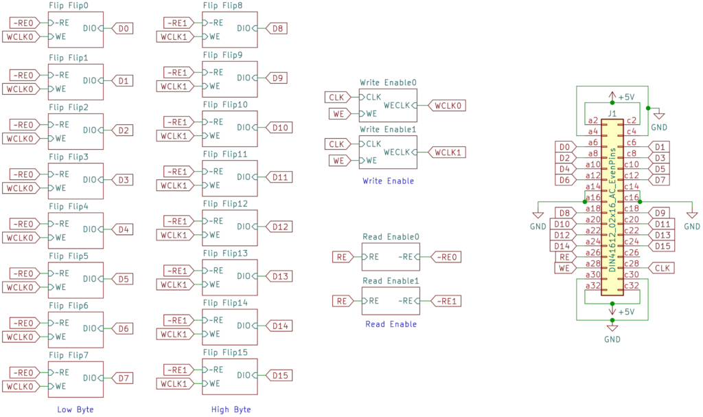
To get the signals in and out, I am using a 32 pin DIN41612 connector that can plug into any carrier board that needs a register like this.

I think this is a nice initial layout for the 16 bit Register Module on an Eurocard PCB. And it would have been a nightmare to set up without the Replicate Layouts Plugin for KiCAD.
Conclusion
For some reason, having the first module for the DWMC-16 sitting in front of me on the screen makes the entire project a little more real for me, as does the new Logo for the project.
But I am sure that someone is going to point me to problems with the schematic and the layout, something that means that I am going to remake the entire thing.
But that is the price to pay for wanting to build this thing.
With this done, I need a few specialised Register Modules. For example, a module for the Registers that go into the ALU, where I do not need a tristate stage, and another module for the Test Register and the Flag Register.