This post will be part of a proper document after the design phase.
Basic Design
This section contains informations about the basic design and design goals of the DWMC-16.
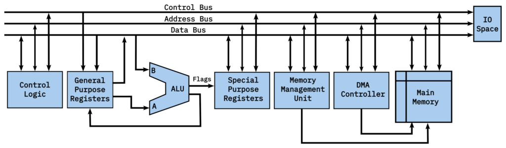
Be basic design is going for a 16 bit Von Neumann machine with a 20 bit address bus, utilizing a Memory Management Unit to support larger sizes of memory, switching the upper 512kiWord of memory be between processes as needed. In a basic memory layout, this allows for 1MiWord (1Mx16) memory, divided into 16 64kiWord sectors.
It also contains a DMA Controller, which can operate in cycle stealing mode, when the CPU does not need to access the data bus, as well as in dedicated mode, when the CPU hands over control over the data and address bus for a longer time. It will have at least two channels available for operation, one channel for transferring data between an IO device with a FIFO buffer, or between two sectors of memory. This includes other memory pages in conjunction with the MMU.
The CPU itself will integrate an Interrupt controller with 7 logical interrupts. These Interrupts are connected to a small FIFO, allowing the system to handle several Interrupts, before returning to the main program.
IO devices are mapped into one sector of memory. In itself the IO sector will be subdivided by the IO modules. Each IO module can take from 1kiWord to 4kiWord of memory, with most of the memory space taken up by an integrated ROM area containing for drivers needed to access the IO module, written to confirm to an API used by the systems OS. Without any additional modules, a basic ‘Blinkenlights’ IO module with several different IO methods will be available. This module will include a basic blinkenlights setup with toggle switches for IO, an Intel 8279 with an 8 digit 7 segment display and an n-key keyboard, as well as a parallel LCD/VFD.
- 16 bit Von Neumann architecture
- Small instruction set, 16 bit wide + addressing
- 20 bit wide address bus (1MiWords, 1Mx16), organized into 16 64kiWord sectors.
- Memory Mapped IO
- Memory Management Unit
- 2 channel DMA Controller
- 7 logical Interrupts
- Build using TTL 74LSxxx logic ICs for hardware
CPU Features
The CPU itself is going to be a Register to Register design, optimized for fast load and store operation and to use a little operation cycles as possible to speed up operation of the system.
It will integrate sixteen 16 bit general purpose registers, R00 to R15, which are are doubled by a second set of sixteen 16 bit registers, R00′ to R15′ that are switched out when the CPU gets an interrupt, allowing for very fast handling of Interrupts without having to involve the Stack Register to save 16 registers. This feature is inspired by the Z80.
The Special Registers, the Program Counter, Stack Pointers, Index Registers and Flag, are mapped into memory, allowing for easy access without having to resort to additonal commands or reducing the number of general purpose registers.
The ALU will also include the ability to execute bit tests non-destructively, as well as setting and resetting single bits.
- Register to Register architecture
- Load/Store optimized architecthre
- Short Operation Cycle optimized
- Two sets of 16x 16 bit general purpose registers
- Special Registers are mapped into low memory
- Non-destructive bit tests (done by the ALU)
Memory Mapping
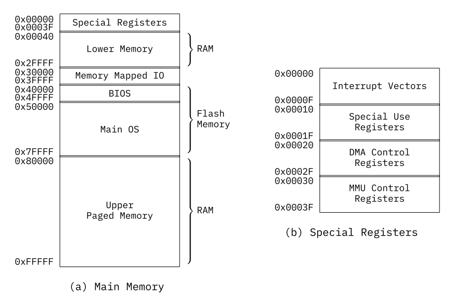
The DWMC-16 is meant to be, in its basic form, able to address 1 MiWord of Memory, using its 20 bit wide address bus.
The memory itself is subdivided into 64 kiWord Sectors, mostly for ease of addressing when operating in a local memory area, allowing for shorter OpCode and shorter programs by splitting addressing into local addressing for work in the local Sector, as well as global addressing to work in the entire memory space.
Additionally, with the use of the Memory Management Unit, the upper 512 kiWord ()8 sectors) can be paged, allowing to swap out the entirety of the 512 ki Word of memory. The lower 512 kiWord of memory are static, which is split as well. The upper 256 kiWord (4 sectors) are taken up by Flash ROM/EPROM memory containing both the BIOS of the system, as well as a basic Monitor OS, as well as the Main OS. Just ahead of the ROM area is the Memory Mapped IO sector of 64 kiWord, used by the system for all forms of IO.
This leaves 192 kiWord (3 sectors) of Lower Static Memory for general use, as well as use by the systems OS. However, the lowest/first 64 Word of Memory are taken up by Special Registers.
This Special Register Space is split into four parts of 16 Words, used for addressing the Interrupt Sectors and Special Use Registers (Program Counter, Index Registers, etc), as well as the Control Registers for both the DMA Controller and the Memory Management Unit.
1 Comment