You will certainly now ask, ‘Why are you already jumping to the ALU?’ Because my brain wants to take care of the ALU first, largely for reasons of interest. Besides, having a design of the ALU allows me to have an idea what operations it can do, once I go for creating the instruction set.
For the most part this post will follow my thought process in how I have designed the initial ALU, from almost the ground up. For this, I am using a program called Digital, which is a slightly more usable and modern version of the venerable LogiSim.
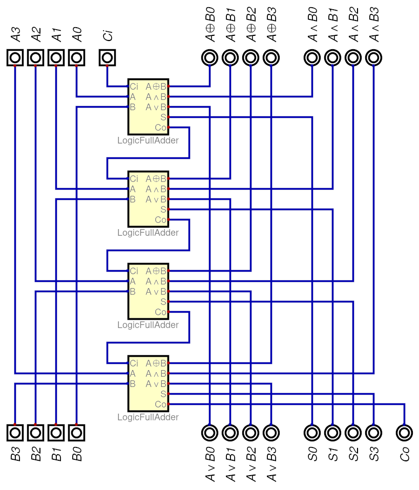
First Step: The Logic Full Adder
We start with a very basic design element for ALUs, the full adder.

Let’s take a look at this schematic and what do I see? Two logical operations that I can access without adding to its complexity, aside from two more connections.
$ A\wedge B $ and $ A\oplus B $. Two of the four important logical operations in a CPU. And by simply adding an OR gate, $ A\vee B $ can be added to this diagram, making it what I call a Logic Full Adder. The $ Ā $ operation will be added later on.

Second Step: 4 bit Logic Adder
By simply chaining four of these Logic Full Adders, we get a diagram of a circuit that can add two four bit numbers, with carry bit, and logically combine them. Which gives $ A\wedge B $, $ A\vee B $ and $ A\oplus B $.
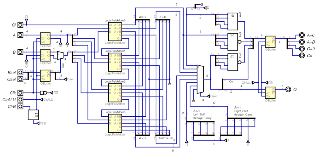
But that isn’t to clean if we turn it into a sub circuit. To reduce the outputs, we can simply add a 8 by 5 bit multiplexer. Why 8 by 5 bit? Glad you asked…
For one we add the $ Ā $ operation into the multiplexer. And then we put the Carry Out bit into bit 5 of the $ A+B $ output for the multiplexer. That of course means that for the other four operations we need to set bit 5 to 0.

Now we have three inputs for the multiplexer left, and we can do something with those. For one, we can easily and with minimal additional complexity add simple 1 bit right shift and left shift operations through carry. Which is why we have added the carry bit into the multiplexer.
And finally we can pull the last input of the multiplexer to 0, for some ALU operations that do not require an output.

| Operation | Osel2 | Osel1 | Osel0 |
|---|---|---|---|
| $ Ā $ | 0 | 0 | 0 |
| $ A\oplus B $ | 0 | 0 | 1 |
| $ A\vee B $ | 0 | 1 | 0 |
| $ A+B $ | 0 | 1 | 1 |
| $ A\wedge B $ | 1 | 0 | 0 |
| $ A<<1 $ | 1 | 0 | 1 |
| $A>>1 $ | 1 | 1 | 0 |
| 0 | 1 | 1 | 1 |
Third Step: Comparing Bits
And those operations that do not require a normal output? Easy comparisons.
In this case we can do three comparisons with adding just three gates.
One would be $ A=0 $, which just required the addition of a single AND gate, with it’s inputs $ Ā $.
The second is $ A=B $, which is just a single NOR gate, with it’s impots being $ A\oplus B $.
And finally $ O=0 $, which is uses another NOR gate in the output signals.

Of course, since these comparisons are made with every operation, they allow for a branch operation like branch if zero, where the CPU branches when the previous operation was zero. Very useful for counting loops.
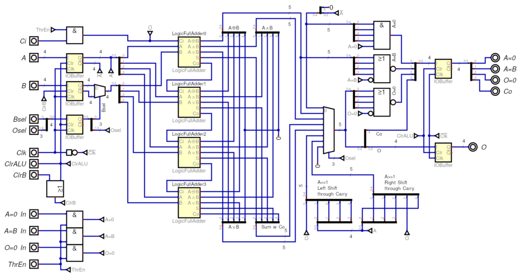
Fourth Step: Input & Out Buffers
Now, I want to put this ALU into an instruction pipeline, and for that, I need to buffer the inputs and outputs. The buffers themselves will just be simple D-Flip-Flops with an additional Reset input. In this case, I will put them into a sub module, buffering four inputs/outputs.

And this makes clear why I didn’t add inverters to get the $ Ā $, since the buffer automatically generates it. Additionally, it also generates a $ \overline{B} $, which can be used as 1-Complement. If combined with a carry bit, it’s easy substraction. It will need a switch/multiplexer to switch between those, though.

The input buffers are loaded on the rising edge of the clock signal, while the output buffers are loaded with the falling edge, allowing the circuit to properly propagate the results through.
Fifth Step: Increment and Decrement
As the logic now stands, it can easily add A to B and substract B from A, the latter two with the use of the carry bit.
But I also want to do an easy decrement of A by 1.
To do this, I need to be able to clear the input buffer for B independently from the clear signal for the entire ALU, which can be achieved by adding an OR gate.
| Operation | Osel2 | Osel1 | Osel0 | Bsel | ClrB | Ci |
|---|---|---|---|---|---|---|
| NOT A | 0 | 0 | 0 | 0 | 0 | 0 |
| AND A,B | 0 | 1 | 0 | 0 | 0 | 0 |
| OR A,B | 1 | 0 | 0 | 0 | 0 | 0 |
| XOR A,B | 0 | 0 | 1 | 0 | 0 | 0 |
| SLC A | 1 | 0 | 1 | 0 | 0 | X |
| SLR A | 1 | 1 | 0 | 0 | 0 | X |
| ADD A,B | 0 | 1 | 1 | 0 | 0 | X |
| SUB A,B | 0 | 1 | 1 | 1 | 0 | 1/X |
| INC A | 0 | 1 | 1 | 0 | 1 | 1/X |
| DEC A | 0 | 1 | 1 | 1 | 1 | 1/X |
The 1/X in the above operations logic table means that the Ci input needs to be either 1, for either a single 4 bit adder or the first adder in a chain of multiple adders, while the X means that the adder takes the input from a previous 4 bit adder.
Sixth Step: 4 bit sliced Adder
This means that the 4 bit adder above could be turned into a bit sliced adder, taking several inputs for the three comparison signals, which need to be fed into the comparison gates in this stage, as we already have the Carry In from a previous stage, currently just used for substraction and increment. At the same time, this means that another signal is needed to enable those additional inputs, which can be done by an AND gate for each signal.
Conclusion
I think I have a reasonable attempt for a workable ALU design in the above design, which gave me some ideas about the later design of the instruction set. I certainly have made some simple tests in the program I have used to design this schematic.
It makes me wonder whether I should integrate some simple instruction decoding directly into the ALU, or if that wouldn’t be duplicated work, if I use four of these babies as the ALU of the DWMC-16s CPU.